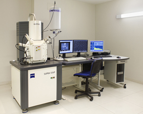
Scanning Electron Microscopy
Info: cimemeb@conicet.gov.ar
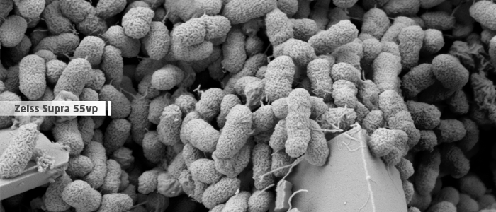
Scanning microscopy images (SEM, Scanning Electron Microscopy) provide a three-dimensional image of the sample surface with a level of detail and depth of field far superior to conventional optical microscopy.
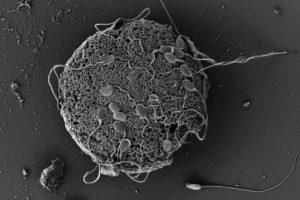
Sample: Cecilia Gramajo - Material: Ovule with sperm
The electron beam, when traveling the sample, starts secondary electrons from it that are captured and converted into lighter or darker tones depending on their intensity. This intensity is directly related to the orientation of the different surfaces towards the collector, so by rotating and tilting the sample we can adapt the direction of the lights and shadows to our liking so that they highlight the most significant details of the sample. -in operation in the CIME- allows the examination of surfaces up to nanometric scales either at high vacuum or at variable pressure (VP, 20 to 40 Pa). It has an X-ray scattering energy spectrometer (EDXS) module for elemental analysis and mapping, a system for orientation of backscattered electron detection (EBSD) crystals, phase mapping using Kikuchi patterns, and the Generation System of nanometric patterns (NPGS), which provides a powerful, versatile and easy-to-use tool for electron beam lithographs.SEM-BSE. The scanning images of backscattered electrons (BSE, Back-Scattered Electrons) form an image of the surface of the sample in which each level of gray is different for each of the elements that form it. The backscattered electrons come from the beam, and are those that are fired by the sample. The probability that these are expelled and reach the detector is directly proportional to the atomic weight of each element present on the surface of the sample. The heavier the element, the more electrons are backscattered and generate brighter areas in the image, and vice versa.
EDXS X-ray energy dispersion microanalysis (EDXS, Energy Dispersive X-ray Spectroscopy) is a fast and efficient technique to detect the elementary composition of a sample at the micro and nanometric level, with a detection range from Boron onwards. A detector captures the x-rays produced in the part of the sample that is tracked or bombarded by electrons, and a digital system relates the different energies and intensities with different elements and their proportions, generating the typical spectrum that can be seen in the image. The electron beam control allows analysis of areas, lines, points, multipoint and mappings, providing valuable compositional information when interpreting images.